
Five gates. Fixed scope at each. Exit at any one.
Each gate has a fixed scope, its own price and a list of files you receive. At the end of each, you decide: continue, adjust, or stop and take everything with you.
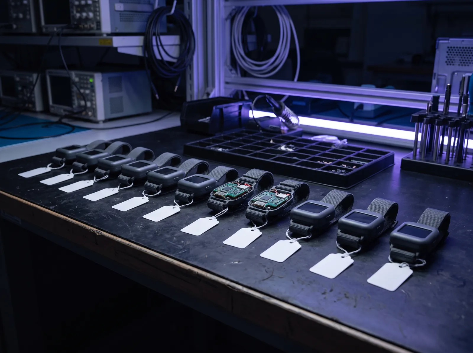 Illustration
Every gate at a glance
Durations and unit counts are typical ranges. Each statement of work gives your dated plan.
- Gate 0
Feasibility
- You get
- System architecture document; Costed BOM with landed DDP estimate
- Yours at this gate
- The architecture, BOM estimate and certification plan, yours to take anywhere.
- Exit
- Stop here and keep every document. Fee is credited if you continue.
- Gate 1
Works-like prototype
- You get
- 3–5 working units shipped to you; First firmware in your repository
- Yours at this gate
- Schematics, layout source and firmware source for the prototype.
- Exit
- Stop and keep the units and all source files.
- Gate 2
EVT · first custom PCB
- You get
- 10–30 looks-like / works-like units; Schematics, layout source, Gerbers, BOM with alternates
- Yours at this gate
- Every electrical, mechanical and firmware file for the EVT design.
- Exit
- Stop and take the full design package to any factory.
- Gate 3
DVT / PVT · small batch
- You get
- 50–1,000 near-final or sellable units; Reliability and pre-scan reports
- Yours at this gate
- Molds and fixtures you paid for, labeled with your name. Certification grants in your name.
- Exit
- Move production to a factory of your choice with molds, fixtures and test procedures.
- Gate 4
Mass production
- You get
- QC report with every lot; DDP shipments to your door
- Yours at this gate
- Everything above, plus lot-level quality records.
- Exit
- Transfer to another manufacturer with a documented handover.
A decision with evidence on the table
Each gate ends with a review: hardware, measured numbers, open risks and files. We give a written go, adjust or stop recommendation. The decision is yours.
Fixed scope and price
The statement of work lists work items, deliverables, pass criteria and a fixed fee before the gate starts.
Files at every gate
Source files and reports are handed over when the gate closes. IP is assigned to you once it is paid.
How ownership works →A real exit
Stop at any gate and keep everything you paid for. You owe nothing for gates you did not start.
Engagement terms →Feasibility: find out if it works before you buy hardware
The wrong module, a battery that cannot last a shift, or a radio that triggers an unplanned certification. Gate 0 settles those choices on paper, where they cost hours.
Questions it answers
- Silicon
- Can your model run on the device, or must audio stream to the cloud?
- Battery
- Will it last a full shift on a battery that fits the enclosure?
- Radio
- LTE-M, Cat-1bis or Wi-Fi plus phone? Which US bands and carriers?
- Modules
- Is the module safe for a US product in 2026, and is there a non-China alternate?
- Cost
- What does it cost per unit, landed in the US, at your target volumes?
- Certification
- Which rule parts apply, which lab, how long, and what fee range?
- Typical duration
- 1–2 weeks
- Hardware built
- None
- Price
- Fixed fee, quoted after a free call. Credited against the next gate if you continue.
- Yours
- The architecture, BOM estimate and certification plan, yours to take anywhere.
- If you stop
- Stop here and keep every document. Fee is credited if you continue.
- To start
- A slide, a sketch or a dev-kit demo is enough. NDA first if you want: mutual NDA.
| You receive | What is in it |
|---|---|
| Architecture document | Block diagram, SoC, radio, sensor and power choices with reasons, data flow, where keys live. |
| Requirements list | Each requirement with a target number, a test method and an owner. |
| Costed BOM + landed DDP estimate | MPNs, alternates, lead time, country of origin; freight, duties, tariffs and brokerage at your volumes. |
| Certification path | FCC rule parts, RF exposure approach, module grants relied on, PTCRB / carrier steps, lab and fee range. |
| Risk register | Each risk with likelihood, impact and the cheapest test that retires it. |
| Fixed quote for the next gate | Scope, deliverables, pass criteria, dated plan and price. |
Every file is editable, so your team or another firm can quote from it. We do not need your model weights or cloud code, only the model’s size, memory, latency target and the API the device talks to.
From proven modules to your first custom PCB
Gate 1 puts your model on the target silicon fast. Gate 2 turns it into a fully custom board and first enclosure. You hold working units and every source file after each.
Works-like prototype
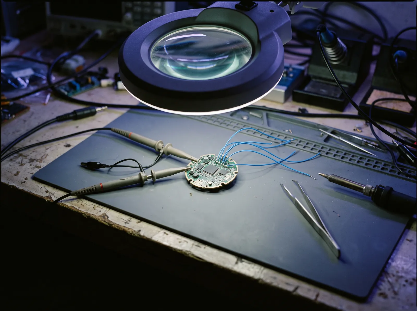
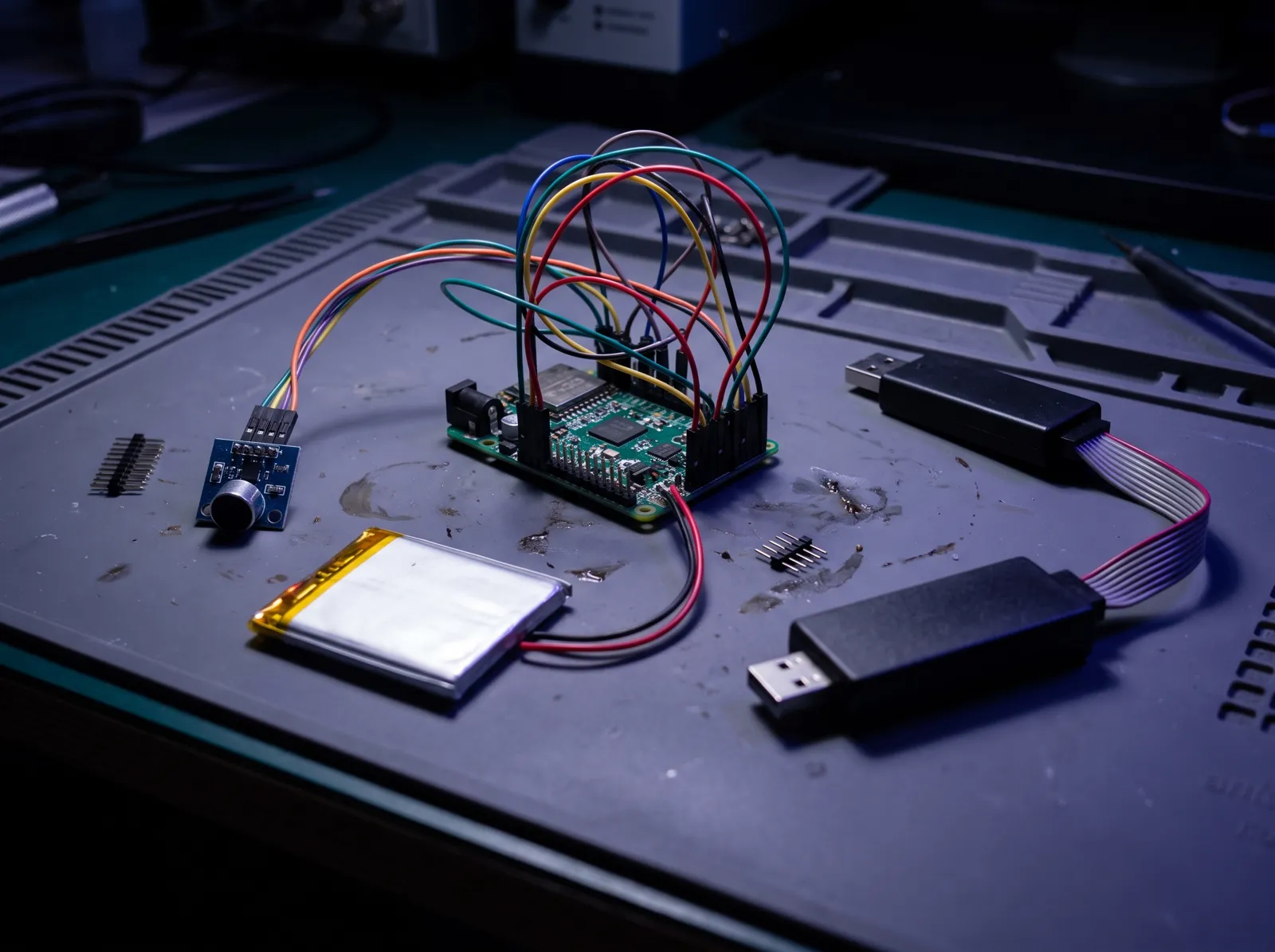
Proven modules on a custom carrier board, so your model runs on the target silicon. It does not look like your product. It runs your model, measures power and talks to your backend.
Exit: Stop and keep the units and all source files.
EVT · first custom PCB
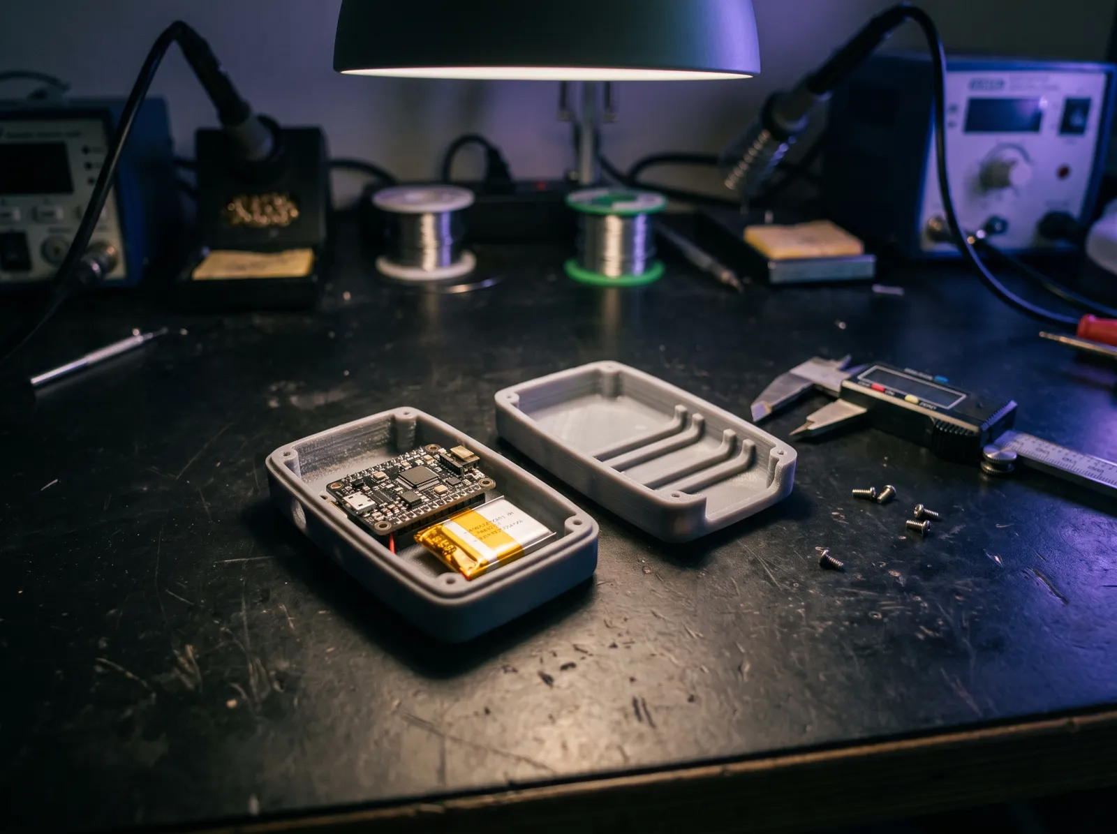
Fully custom schematic and layout, bring-up, first enclosure, firmware with OTA and provisioning. Provisioning keys stay under your control.
Exit: Stop and take the full design package to any factory.
| Deliverable | Gate 1 | Gate 2 · EVT |
|---|---|---|
| Units | 3–5 works-like units on a carrier board | 10–30 looks-like / works-like units in the first enclosure |
| Schematic + layout | Carrier board: native files, PDF, Gerbers | Full custom: native files, stack-up, Gerber or ODB++, drill, netlist, pick-and-place |
| BOM | MPNs, modules and dev kits used | MPNs, approved alternates, lifecycle, lead time, country of origin |
| Mechanical | — | STEP and native CAD, 2D drawings with tolerances |
| Firmware | First firmware in your Git repo, pinned toolchain | Bootloader, OTA, provisioning, reproducible build, SBOM |
| Report | Measured power, model latency on target silicon, RF numbers | EVT test report: bring-up, battery, RF, EMI pre-scan, thermal, drop, ESD |
| Decision | Go / adjust / stop memo, fixed EVT quote | Fixed Gate 3 quote, including tooling |
You get native CAD files plus neutral formats any team can open. Can you skip Gate 1? Sometimes, if Gate 0 shows the silicon and radio are already proven. EVT, DVT and PVT explained.
 Illustration
 Illustration
 IllustrationIllustration
Small batches on a real production line
Many prototype shops stop at a few dozen units. Many factories set minimums in the thousands. Gate 3 covers the range in between.
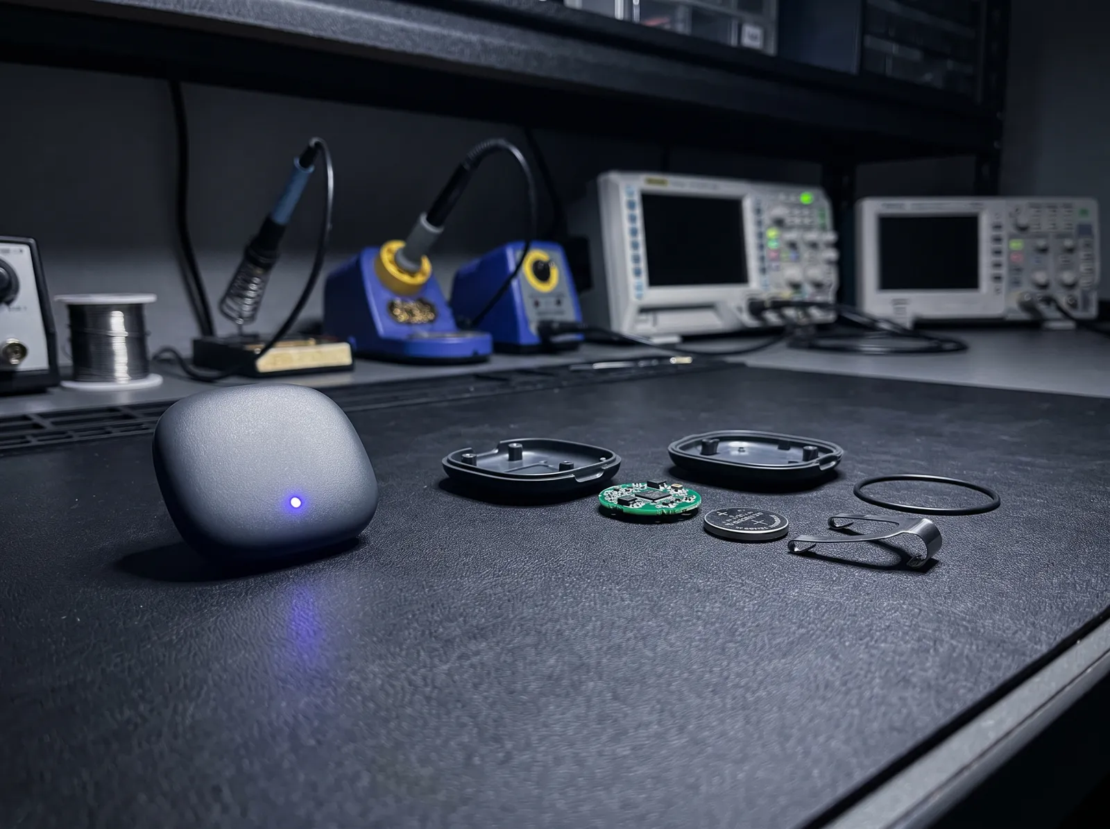
- DVT proves the final design passes reliability tests and RF pre-scan.
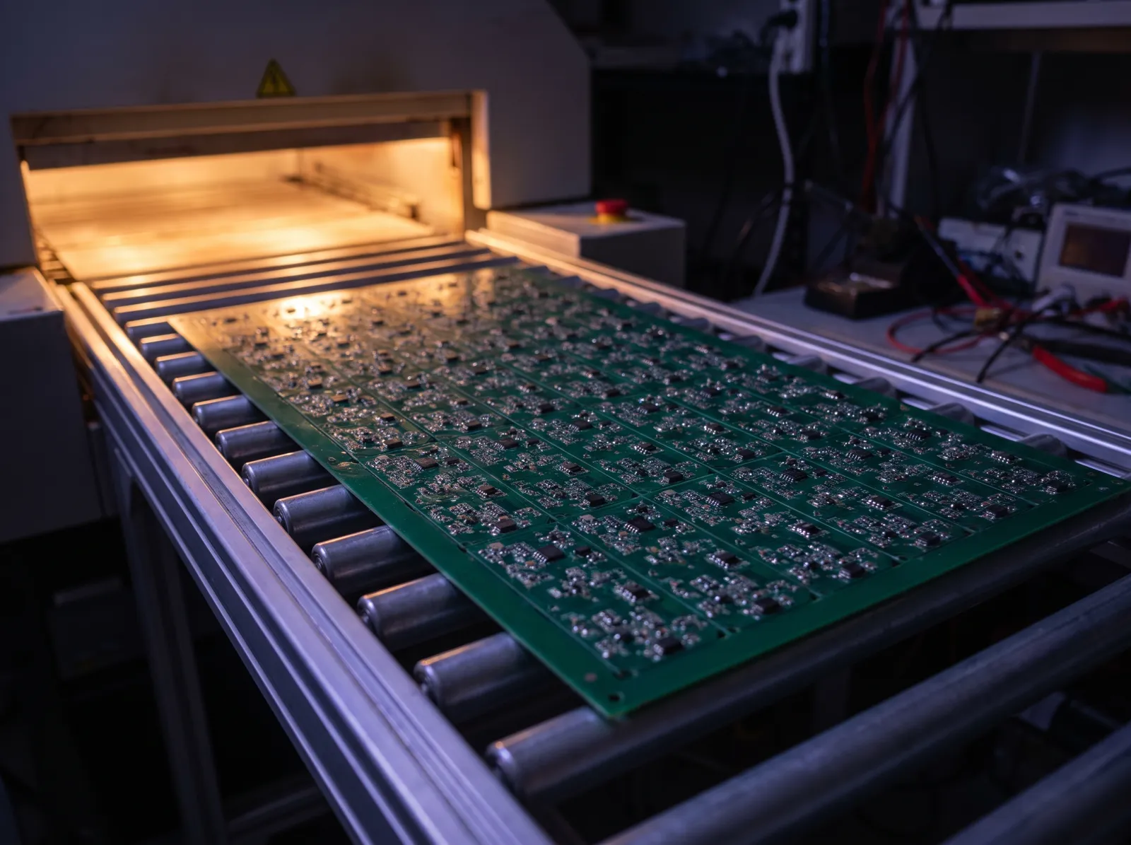
- PVT proves the line, fixtures and test procedure build it at yield. Small projects may merge the two; the SOW says which.
- Certification in your name. Formal FCC testing on DVT/PVT units, with your company as grantee.
- Shipped DDP to your US address, warehouse or 3PL.
What you receive
- Locked BOM with second sources and an approved vendor list
- Final design package at the released revision
- Reliability report (DVT) and RF pre-scan report
- FCC test reports and grant in your company’s name; PTCRB / carrier approvals if cellular; UN38.3 for the battery
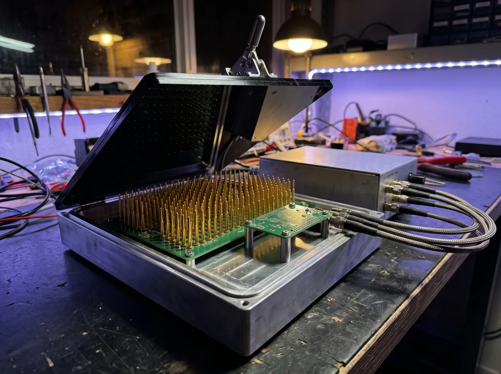
- Test fixtures, production test software source and station-by-station procedure
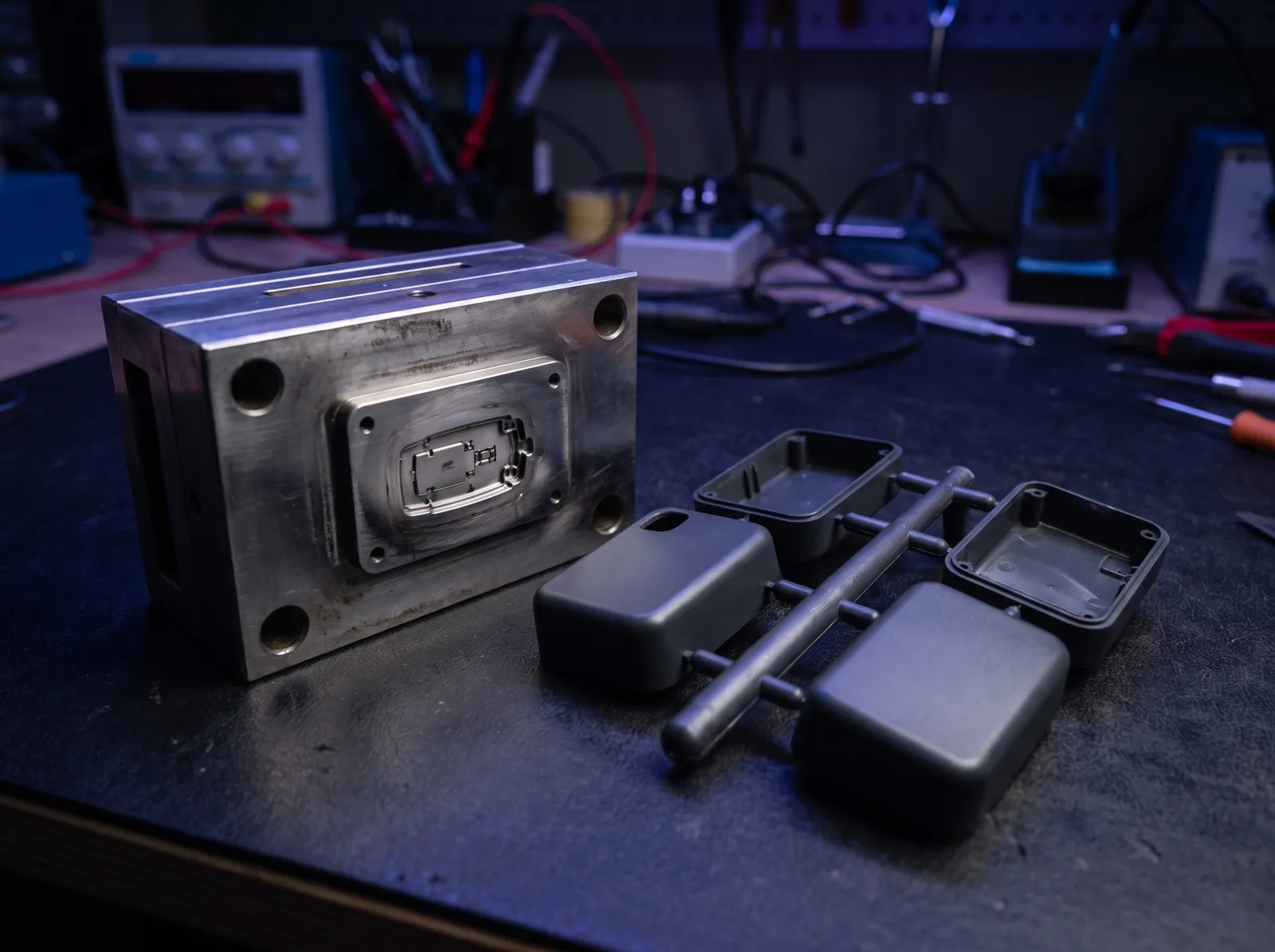
- Tooling records with photos of your name and asset number on each mold
- Yield report, tagged production firmware release, packaging and label artwork
With this package and your tooling, a second factory can build your product without us.
 Illustration
 Illustration
 Illustration
 Illustration
Steady production, landed at your door. Or a clean handover.
The design is locked and certified. The work shifts to forecast, supply, quality and delivery, and to taking cost out without touching what was certified.
What we run
- Material planning against your rolling forecast
- Buffer stock of critical, long-lead parts
- Incoming, in-process and outgoing inspection on every lot
- Production test on every unit, provisioning with keys you control
- DDP shipping: export, freight, US customs entry, duties, delivery
- Change control and end-of-life monitoring on the BOM
What you receive
- Lot QC report with every lot, against the agreed AQL sampling plan
- Traceability: serial to lot, lot to critical component batches
- Shipment documents and a landed cost statement matched to the quote
- End-of-life and lead-time alerts with a proposed alternate
- Change records with certification impact
- Quarterly cost-down review
Moving to another factory
Transfer to another manufacturer with a documented handover. The FCC grant stays yours as long as the new factory builds the device identically.
- 1
Notice
You give written notice and name the receiving factory.
- 2
Last lot
We agree the last lot we build and any last-time buy of parts.
- 3
Handover
Design, manufacturing and test packages, quality history and certification file. Molds and fixtures you own are released and shipped.
You pay for lots already ordered and parts bought against your firm forecast window. Notice period, parts outside the firm window and handover support: [Production exit terms — to confirm with counsel].
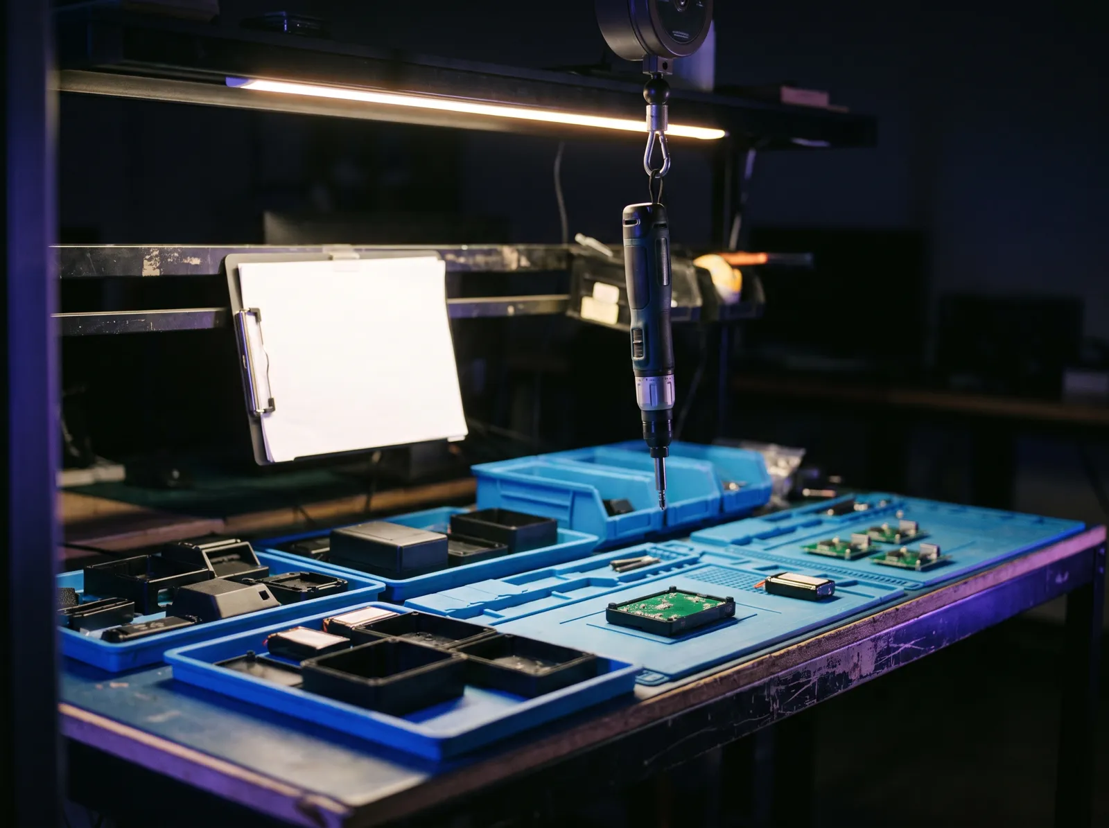 Illustration
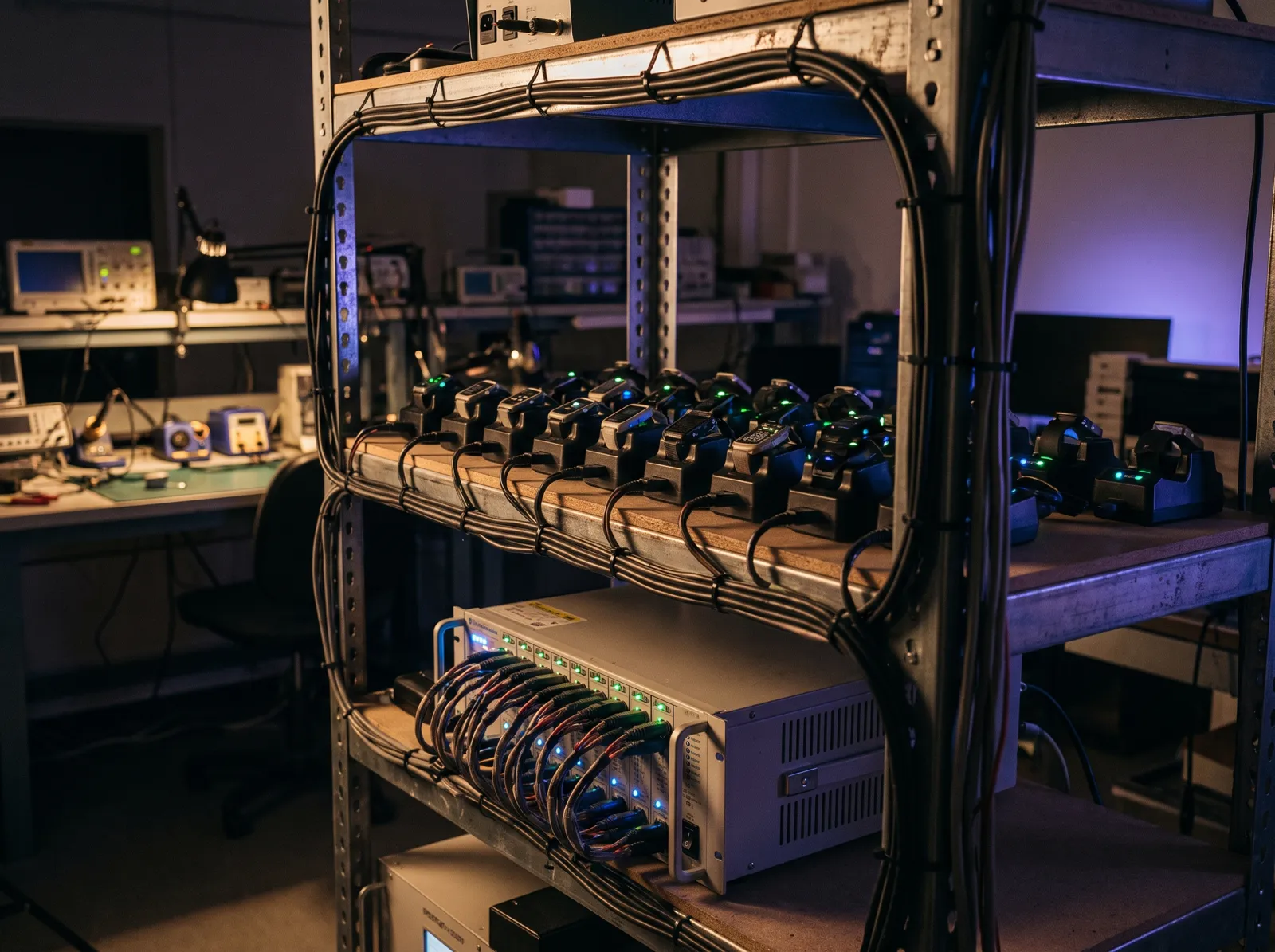 Illustration
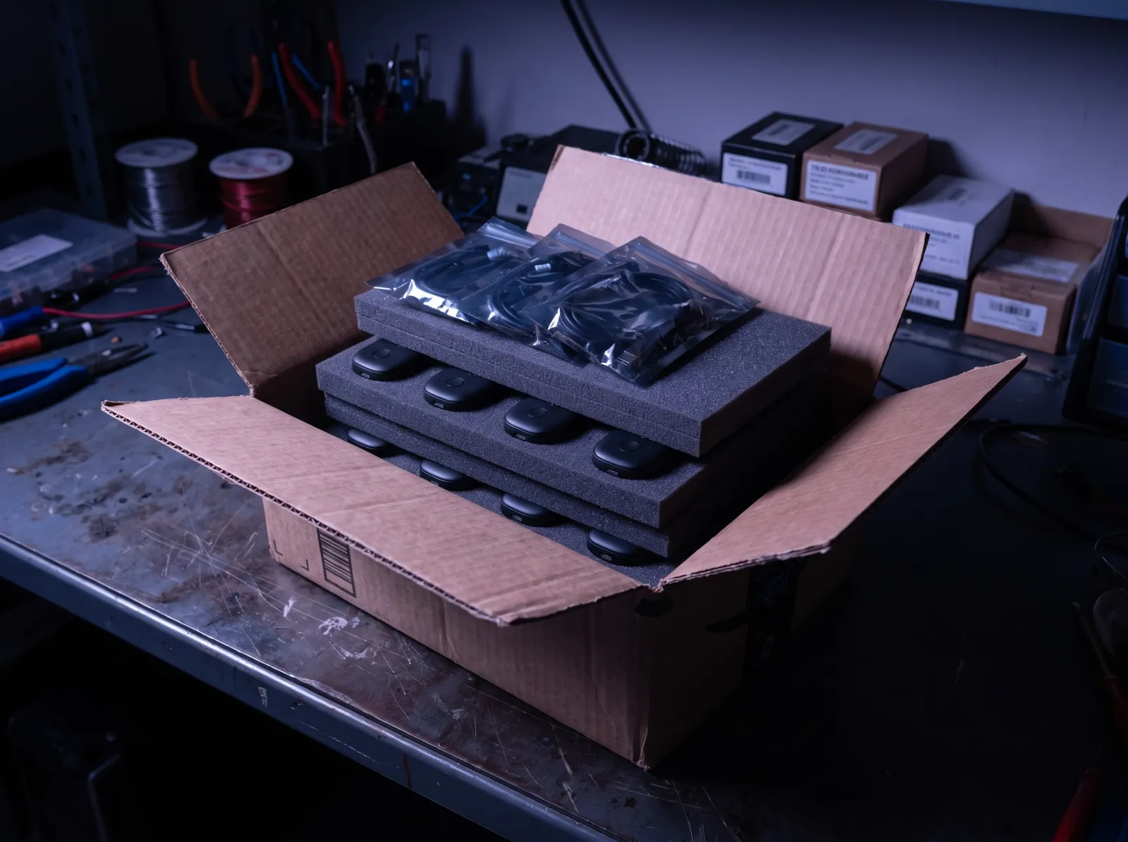 Illustration
One fixed price per gate, quoted before it starts
We do not publish prices, because two devices rarely share a scope. We do publish how a quote is built.
Free
Scoping calls and a first look at your spec or BOM. Reply within 2 business days.
Fixed fee, credited
Paid feasibility study, quoted after a free call. The full fee is credited against the next gate if you continue.
Fixed fee per gate, plus materials
Engineering fee set by scope. PCBs, assembly, tooling and fixtures are itemized. Molds and fixtures you pay for are yours.
Landed DDP price per unit
Unit cost, freight, US duties and tariffs, brokerage and delivery to your warehouse or 3PL.
How DDP pricing works →Paid by you, managed by us
Lab and certification fees are yours. Grants and reports are issued in your company’s name, so they move with you.
Certification approach →Try the estimator
A first range for landed unit cost and the certification path, before any call.
Open the estimator →FCC work at every gate
The path is planned at Gate 0, so certification is a scheduled step with a known lab, timeline and fee range.
| Gate | FCC / certification action |
|---|---|
| Gate 0 · Feasibility | Map rule parts (Part 15B, 15C, 15E, 22/24/27) and the RF exposure approach. Pick pre-certified modules not made by Covered List entities. Plan PTCRB and carrier steps. Name the lab. |
| Gate 1 · Works-like prototype | Use modules only with the antenna types and gains their grants allow. First conducted-power measurements. |
| Gate 2 · EVT · first custom PCB | Antenna tuning in the enclosure, EMI pre-scan, draft test plan with the lab. Register your company as grantee. |
| Gate 3 · DVT / PVT · small batch | Formal testing, grant in your name, SAR or exemption, PTCRB and carrier approvals, UN38.3, FCC ID labeling. |
| Gate 4 · Mass production | Every BOM, antenna or firmware change checked for permissive-change impact. Labels and SDoC records kept per lot. |
As of October 2026. Since December 26, 2025, the FCC does not authorize devices containing modules from Covered List entities (FCC 25-71). We run formal certification testing at FCC-recognized labs outside mainland China, such as Taiwan, Hong Kong or the US. Our certification approach.
The engineers who did the work present it
Electrical, firmware, mechanical and test engineers in Shenzhen walk you through their results. The founder in the Bay Area runs the review. Your contract is with Aximora Labs Inc., a US company.
Your cloud, your keys
No China-hosted cloud in the data path. Provisioning keys are yours. Firmware source is in your repository from Gate 1, and an SBOM ships from EVT on.
Questions about the gates
Do we have to start at Gate 0?
Usually yes. It is short, fixed-fee and credited if you continue. If you already have an architecture, a costed BOM and a certification plan you trust, we review them and quote the next gate directly.
We already have a working PCB. Can we enter at Gate 2 or 3?
Yes. Send the schematic, layout, BOM and firmware. We run a design review, list what we would change, and quote from there. We re-check the certification path, because late surprises often come from antenna and module choices.
What if Gate 0 shows the device does not make sense?
Then you spent a small, fixed amount to learn it before buying hardware, and you keep the documents. A study can end with a recommendation to buy an existing device, change the radio or drop a feature.
What happens if we stop in the middle of a gate?
You tell us in writing, we stop work, and you receive the work-in-progress files. The statement of work sets how the stop is settled: [Mid-gate stop settlement rule — to confirm with counsel]. Engagement terms.
Who owns firmware that uses vendor SDKs?
You own the code we write. Third-party SDKs and open-source components keep their own licenses, and the SBOM lists each one so your counsel can check it. Handover checklist.
Can we give prototype units to real customers?
For internal trials, yes. Before a radio device is authorized, US rules limit marketing and sale (47 CFR 2.803). We plan the build order so sellable units land after the grant.
Do you really build batches as small as 10 units?
Yes. Gate 3 is planned for 10–1,000 units. Below a few hundred units we usually use soft tooling or CNC parts, and quote a steel mold when your volume justifies it.
Who owns the molds?
You do, once you have paid for them. Each mold carries your company name and an asset number, is photographed in the tooling file, and can ship to another factory on request.
Does a factory move affect our FCC grant?
The grant belongs to your company and covers the design, not the factory. If the new factory builds it identically, the grant still applies. Antenna, RF layout or module changes may need a permissive change, so we list what must stay identical.
Are the durations guaranteed?
No. They are typical ranges. Each statement of work gives a dated plan. Long-lead parts, tooling and lab queues are the usual reasons a gate moves, and we tell you as soon as one does.
Can gate reviews happen in person?
Yes, in the San Francisco Bay Area with the hardware on the table, or by video with the Shenzhen engineers. Bay Area reviews.
Next step. An idea, a dev-kit demo, or a board that almost works: tell us where you are and we will say which gate to start at. A Duobay engineer replies within 2 business days.